- 您现在的位置:买卖IC网 > Sheet目录3841 > PIC16F737-I/SP (Microchip Technology)IC PIC MCU FLASH 4KX14 28DIP
2009 Microchip Technology Inc.
DS39636D-page 225
PIC18F2X1X/4X1X
19.2
Comparator Operation
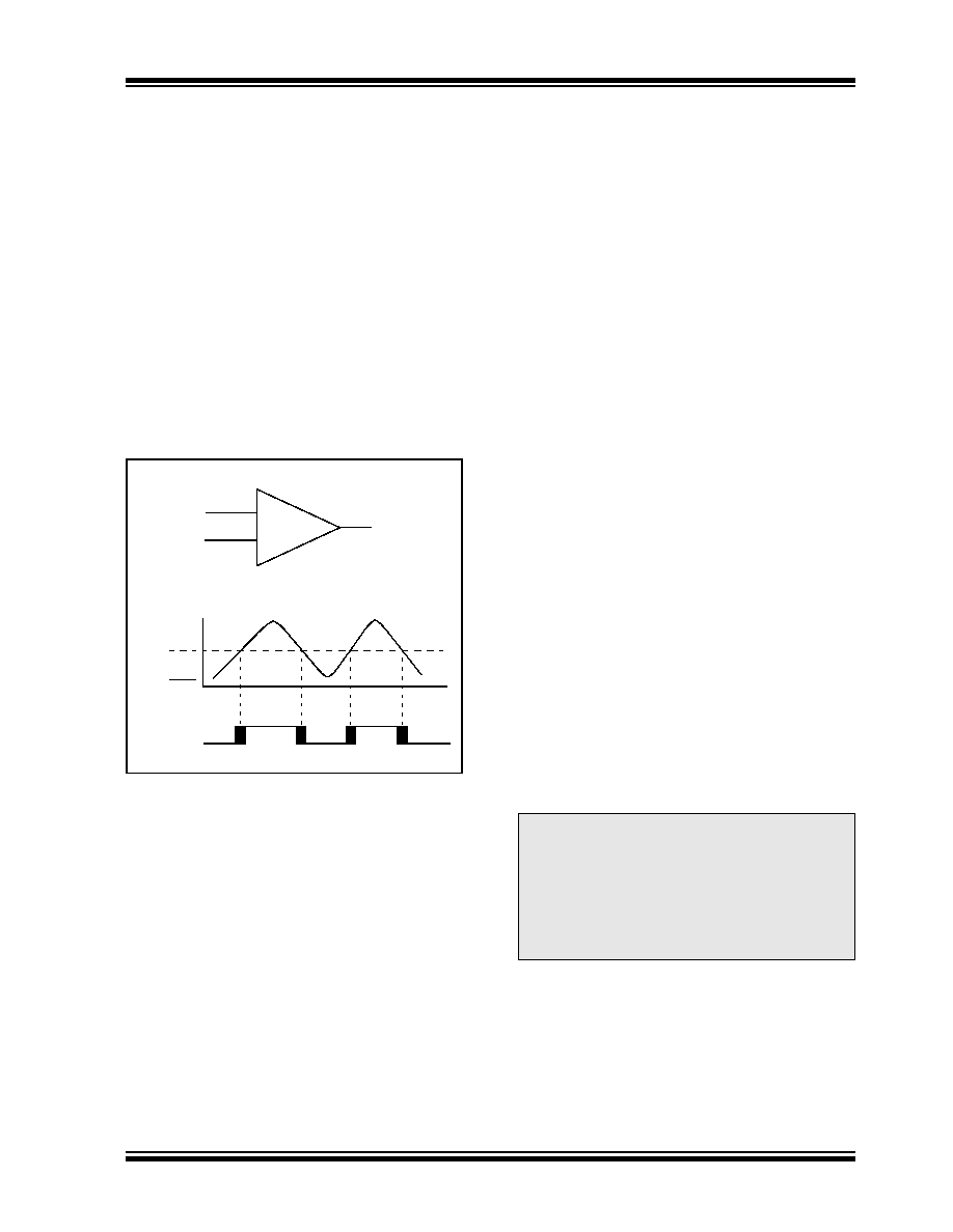
A single comparator is shown in Figure 19-2, along with
the relationship between the analog input levels and
the digital output. When the analog input at VIN+ is less
than the analog input VIN-, the output of the comparator
is a digital low level. When the analog input at VIN+ is
greater than the analog input VIN-, the output of the
comparator is a digital high level. The shaded areas of
the output of the comparator in Figure 19-2 represent
the uncertainty, due to input offsets and response time.
19.3
Comparator Reference
Depending on the comparator operating mode, either
an external or internal voltage reference may be used.
The analog signal present at VIN- is compared to the
signal at VIN+ and the digital output of the comparator
is adjusted accordingly (Figure 19-2).
FIGURE 19-2:
SINGLE COMPARATOR
19.3.1
EXTERNAL REFERENCE SIGNAL
When external voltage references are used, the
comparator module can be configured to have the com-
parators operate from the same or different reference
sources. However, threshold detector applications may
require the same reference. The reference signal must
be between VSS and VDD and can be applied to either
pin of the comparator(s).
19.3.2
INTERNAL REFERENCE SIGNAL
The comparator module also allows the selection of an
internally generated voltage reference from the
comparator voltage reference module. This module is
described in more detail in Section 20.0 “Comparator
The internal reference is only available in the mode
where four inputs are multiplexed to two comparators
(CM2:CM0 = 110). In this mode, the internal voltage
reference is applied to the VIN+ pin of both
comparators.
19.4
Comparator Response Time
Response time is the minimum time, after selecting a
new reference voltage or input source, before the
comparator output has a valid level. If the internal
reference is changed, the maximum delay of the
internal voltage reference must be considered when
using the comparator outputs. Otherwise, the
maximum delay of the comparators should be used
19.5
Comparator Outputs
The comparator outputs are read through the CMCON
register. These bits are read-only. The comparator
outputs may also be directly output to the RA4 and RA5
I/O pins. When enabled, multiplexors in the output path
of the RA4 and RA5 pins will switch and the output of
each pin will be the unsynchronized output of the
comparator.
The
uncertainty
of
each
of
the
comparators is related to the input offset voltage and
the response time given in the specifications.
Figure 19-3 shows the comparator output block
diagram.
The TRISA bits will still function as an output enable/
disable for the RA4 and RA5 pins while in this mode.
The polarity of the comparator outputs can be changed
using the C2INV and C1INV bits (CMCON<4:5>).
–
+
VIN
+
VIN
-
Output
VIN-
VIN+
Note 1: When reading the Port register, all pins
configured as analog inputs will read as a
‘0’. Pins configured as digital inputs will
convert an analog input according to the
Schmitt Trigger input specification.
2: Analog levels on any pin defined as a
digital input may cause the input buffer to
consume more current than is specified.
发布紧急采购,3分钟左右您将得到回复。
相关PDF资料
PIC18F86K22-I/PTRSL
MCU PIC 64K FLASH XLP 80TQFP
PIC16C63A-04I/SP
IC MCU OTP 4KX14 PWM 28DIP
PIC16C63A-04I/SO
IC MCU OTP 4KX14 PWM 28SOIC
52559-2270
CONN FFC 22POS .5MM VERT ZIF SMD
52559-1870
CONN FFC 18POS .5MM VERT ZIF SMD
DSPIC33EP64MC506-I/PT
IC DSC 16BIT 64KB FLASH 64TQFP
52745-1896
CONN FFC 18POS .5MM R/A ZIF SMD
PIC16LC622-04/P
IC MCU OTP 2KX14 COMP 18DIP
相关代理商/技术参数
PIC16F737-I/SP
制造商:Microchip Technology Inc 功能描述:IC 8BIT FLASH MCU 16F737 SDIL28
PIC16F737-I/SS
功能描述:8位微控制器 -MCU 7KB 368 RAM 25 I/O RoHS:否 制造商:Silicon Labs 核心:8051 处理器系列:C8051F39x 数据总线宽度:8 bit 最大时钟频率:50 MHz 程序存储器大小:16 KB 数据 RAM 大小:1 KB 片上 ADC:Yes 工作电源电压:1.8 V to 3.6 V 工作温度范围:- 40 C to + 105 C 封装 / 箱体:QFN-20 安装风格:SMD/SMT
PIC16F737T-I/ML
功能描述:8位微控制器 -MCU 7KB 368 RAM 25 I/O RoHS:否 制造商:Silicon Labs 核心:8051 处理器系列:C8051F39x 数据总线宽度:8 bit 最大时钟频率:50 MHz 程序存储器大小:16 KB 数据 RAM 大小:1 KB 片上 ADC:Yes 工作电源电压:1.8 V to 3.6 V 工作温度范围:- 40 C to + 105 C 封装 / 箱体:QFN-20 安装风格:SMD/SMT
PIC16F737T-I/SO
功能描述:8位微控制器 -MCU 7KB 368 RAM 25 I/O RoHS:否 制造商:Silicon Labs 核心:8051 处理器系列:C8051F39x 数据总线宽度:8 bit 最大时钟频率:50 MHz 程序存储器大小:16 KB 数据 RAM 大小:1 KB 片上 ADC:Yes 工作电源电压:1.8 V to 3.6 V 工作温度范围:- 40 C to + 105 C 封装 / 箱体:QFN-20 安装风格:SMD/SMT
PIC16F737T-I/SS
功能描述:8位微控制器 -MCU 7KB 368 RAM 25 I/O RoHS:否 制造商:Silicon Labs 核心:8051 处理器系列:C8051F39x 数据总线宽度:8 bit 最大时钟频率:50 MHz 程序存储器大小:16 KB 数据 RAM 大小:1 KB 片上 ADC:Yes 工作电源电压:1.8 V to 3.6 V 工作温度范围:- 40 C to + 105 C 封装 / 箱体:QFN-20 安装风格:SMD/SMT
PIC16F73-E/ML
功能描述:8位微控制器 -MCU 7 KB 368 RAM 25I/O RoHS:否 制造商:Silicon Labs 核心:8051 处理器系列:C8051F39x 数据总线宽度:8 bit 最大时钟频率:50 MHz 程序存储器大小:16 KB 数据 RAM 大小:1 KB 片上 ADC:Yes 工作电源电压:1.8 V to 3.6 V 工作温度范围:- 40 C to + 105 C 封装 / 箱体:QFN-20 安装风格:SMD/SMT
PIC16F73-E/SO
功能描述:8位微控制器 -MCU 7KB 192 RAM 22 I/O RoHS:否 制造商:Silicon Labs 核心:8051 处理器系列:C8051F39x 数据总线宽度:8 bit 最大时钟频率:50 MHz 程序存储器大小:16 KB 数据 RAM 大小:1 KB 片上 ADC:Yes 工作电源电压:1.8 V to 3.6 V 工作温度范围:- 40 C to + 105 C 封装 / 箱体:QFN-20 安装风格:SMD/SMT
PIC16F73-E/SP
功能描述:8位微控制器 -MCU 7KB 192 RAM 22 I/O RoHS:否 制造商:Silicon Labs 核心:8051 处理器系列:C8051F39x 数据总线宽度:8 bit 最大时钟频率:50 MHz 程序存储器大小:16 KB 数据 RAM 大小:1 KB 片上 ADC:Yes 工作电源电压:1.8 V to 3.6 V 工作温度范围:- 40 C to + 105 C 封装 / 箱体:QFN-20 安装风格:SMD/SMT